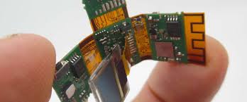
Traces Routed in Rigid-Flex PCB Fabrication
Rigid-flex circuits are used in a variety of applications due to their flexibility, resilience, and temperature resistance. Despite these benefits, rigid-flex PCB fabrication requires careful design and construction to prevent EMI (Electromagnetic Interference) and signal integrity problems.
High-speed signals require tight impedance matching to maintain their performance. Mismatches caused by different copper widths and dielectric materials can cause reflected signals that degrade the quality of the signal. Controlled impedance routing in rigid flex pcb fabrication ensures that trace widths are tightly controlled to maintain a flat impedance profile and avoid EMI.
Differential pairs are used to compare two signals to determine whether they’re in a HIGH or LOW logic state. This eliminates the need for multiple single-ended traces, which reduces power consumption and improves noise rejection. However, differential signaling is more difficult to route than single-ended traces. The length of the traces and their placement within the board can impact the quality of the signal, especially when it bends.
How Are Signal Traces Routed in Rigid-Flex PCB Fabrication?
Using differential pairs in flex PCBs requires that the traces be closely connected and routed together. This reduces power losses and ensures that the logical states of each signal are correctly recognized by the receiver. It also minimizes EMI and ensures that both signals receive the same amount of external noise. However, it’s important to consider the effects of signal length on flex circuit performance and to keep track of the rise time and impedance requirements for differential signaling.
The layer stack-up of a rigid-flex circuit is a critical part of the design process because it determines how easily the flexible portion of the circuit can be bent and folded. For example, thicker layers require larger bending radiuses than thinner layers. The layer stack-up also affects how easy it is to place components on the flex section.
The topmost layer of the flex section of a PCB is typically made of a polyimide substrate film, which allows the traces to be routed and soldered onto it. The substrate is covered by adhesives and other layers, which help it withstand the stresses of mechanical bending. Depending on the application, the flex circuit may be enclosed in a stiffener, which provides additional support.
To make a via, a copper pad is placed at a specific location on each layer of the flex PCB. Holes are drilled through the copper pads on all the layers of the flex PCB, and they’re then plated with conductive material to establish electrical connections between the layers. Once the vias are plated, they’re cleaned with chemicals to remove burrs and epoxy residues before the rest of the PCB undergoes an electroplating process.
A flex PCB can use several types of shielding, including reference plane layers and metal-to-metal contact (MTC). Reference plane layers help to reduce electromagnetic interference (EMI) by eliminating signal reflections and improving impedance control. They can be made of either a microstrip or stripline geometry, with microstrip being thinner and having a narrower core. The stripline geometry is much thicker, which increases the bending tolerance. A flexible PCB can also utilize a coverlay or bondpile, which are flexible materials that insulate and protect the flex circuitry on surface areas and prevent it from lifting.